Integrated Motor Drive Using Paralleled GaN HEMTs on Extreme Copper Printed Circuit Boards for High Temperature Operation
CEME Collaborator Professor Bulent Sarlioglu with Research Assistant
Woongkul Lee – University of Wisconsin-Madison
Compact and energy-efficient integrated motor drive (IMD) applications require a high-power-density inverter. A gallium nitride (GaN) high electron mobility transistor (HEMT) has a lateral device structure with a land-grid array or ball-grid array package for minimum parasitic inductance and resistance, as well as for thermal management. This research project, supported by the Grainger Center for Electric Machinery and Electromechanics, presents a new thermal management methodology for a high-power density IMD using parallel GaN HEMTs. Four PCB design parameters (copper thickness, area, distance between devices, and via pitch) are considered to improve thermal performance and reduce parasitic inductances. It is found the optimized PCB layout with heavy copper (> 2 oz/ft2) and wide copper area (>2.5 in2) can significantly improve the thermal performance of GaN HETMs without any additional heat sink or forced-air cooling system.
Three different half-bridge inverter prototypes with different copper areas are designed and tested (see Figure 1) to verify the effectiveness of the proposed cooling method in a GaN HEMT-based IMD application. Thermal performance analysis results show that the top device temperature is reduced by 11.9 °C in prototype C as compared to prototype A and the bottom device temperature is reduced by 8.9 °C in prototype C as compared to prototype A. The images taken by FLIR E50 infrared thermal imaging camera show that heat generated from both top and bottom switches is dissipated through the copper traces (see Figure 2). They prove the effectiveness of the proposed cooling method. This research study allows the GaN HEMT-based IMD system to be more compact and efficient, and this technology is readily applicable for other power electronics application for better thermal performance and higher power density.

Fig. 1. Populated GaN HEMT-based non-isolated point-of-load synchronous buck converters (prototype A with 2.16 cm x 2.16 cm copper area, B with 2.67 cm x 2.67 cm copper area, and C with 3.18 cm x 3.18 cm copper area from top to bottom).
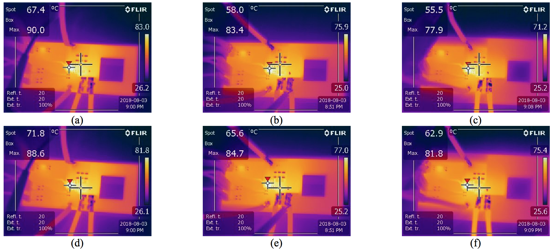
Fig. 2. Measured device case temperature with output current of 5.3 A. (a) top switch in prototype A, (b) top switch in prototype B, (c) top switch in prototype C, (d) bottom switch in prototype A, (e) bottom switch in prototype B, (e) bottom switch in prototype C.