Improved DC Performances of GaN-Based High-Power Field-Effect Transistors Due to Low-Resistance Ohmic Contacts
Stanley Hong and Chandler Seo with adviser Kevin Kim

Figure 15: Schematic diagrams of GaN planar HEMT (HEMT-A), recessed-gate HEMT (HEMT-B), and recessed-source/drain HEMT (HEMT-C).
Previously, we have reported recordhigh peak drain current and maximum transconductance of GaN metal-semiconductor field-effect transistors (MESFETs) using a selective-area-growth (SAG) technique performed by plasma-assisted molecular beam epitaxy (PAMBE). The PAMBE- based SAG enabled selective growth of heavily doped n+-GaN layer (1.0 × 1019 cm-3) only for source/drain regions, giving rise to extremely low contact resistivity (1.8 × 10⁻⁸ Ω∙cm2) for MESFET devices. We extended the advantage of this technique to AlGaN/GaN high electron mobility transistors (HEMTs) and investigated the effect of PAMBE-SAG on the dc performance of HEMT devices.
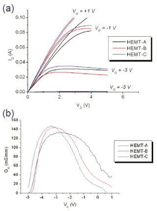
Figure 16: I-V (a) and transfer characteristics (b) of HEMT-A, HEMT-B, and HEMT-C.
In this study, we fabricated planar, recessed-gate, and recessed-source/drain GaN HEMTs, as illustrated in the schematic diagram of Figure 15 (HEMT-A, HEMTB, and HEMT-C, respectively). The gate length, width, and source-to-drain spacing were 1 μm, 200 μm, and 4 μm, respectively. As shown in the dc characteristics of Figure 16, HEMT-B exhibited much higher drain current, lower on-state resistance, and higher transconductance than HEMT-A because the contact resistance was reduced from 5.2 × 10⁻⁵ Ω∙cm2 to 1.6 × 10⁻⁶ Ω∙cm2 due to the use of SAG structure. HEMT-C showed further enhanced dc performance, indicating that the series resistance of the channel was reduced when the AlGaN layer under source/drain regions was dry-etched and the SAG structure grew in direct contact with the 2-dimensional electron gas channel. We believe that the advantages of PAMBE-SAG, such as low temperature growth and ensured Si-doping just underneath the metal contacts, can facilitate fabricating more reliable ohmic contacts for high-power GaN-based FET devices.
For this research, two graduate students, Stanley (Seung Jae) Hong and Chandler (Huichan) Seo, are working together on film growth, device process, and device characterization.