High-power Operation of AlGaN/GaN HEMTs Achieved by PAMBE-SAG and SiO2 Gate Insulator
PhD student Liang Pang with Adviser Kyekyoon (Kevin) Kim, Thin Film and Charged Particle Research Laboratory
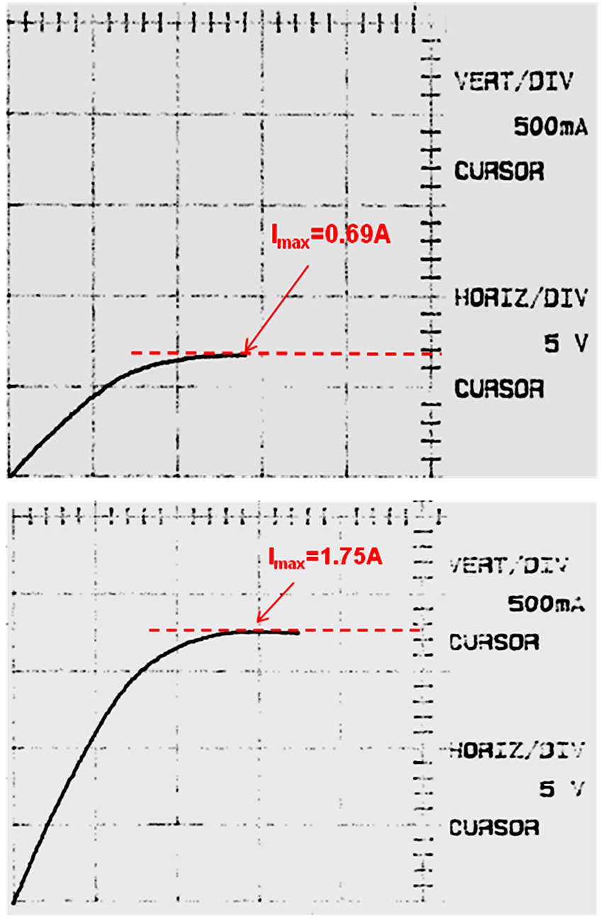
Figure 15: (a) I-V characteristics of five device units interconnected by wire bonding, and (b) I-V characteristics of thirteen device units interconnected by wire bonding (Total Wg = 5.2 mm).
There are three key challenges in developing GaN-based devices for power-switching applications: achievement of low on-state resistance, high current density, and high breakdown voltage. We previously reported that selective-area growth (SAG) by plasma-assisted molecular beam epitaxy (PAMBE) is able to improve contact resistance and current density over conventional contact schemes including ion-implantation. A twofold increase in the breakdown voltage also shows that unlike ion-implantation, SAG does no harm to the device breakdown behavior. In this study, SAG was employed to fabricate high electron mobility transistors (HEMTs) for high-current operation.
A single device unit processed via SAG showed a current of over 0.1 A, more than twice that of the one without SAG. Significant improvement of specific on-state resistance was also observed. A current level of 0.69 A was demonstrated when five device units were interconnected (Figure 15(a)). A linear relationship between the unit number and the current level was found. A maximum current of 1.75 A was achieved for a total gate width of 5.2 mm (interconnection of 13 device units shown in Figure 15(b)). The resulting current density was higher than many previously reported values, demonstrating that the same current level can be achieved with a smaller footprint when SAG is employed.
A new technique for depositing SiO2 as the gate insulator was developed for breakdown voltage enhancement. The breakdown measurement showed a low leakage current of 5 × 10⁻⁶ A/mm at a reserved gate bias of -130 V and a maximum Schottky gate breakdown voltage of 360 V. The three-terminal off-state breakdown voltage was as high as 630 V. The 630 V breakdown voltage at a gate-drain-distance of 6 μm is higher than the MOSHEMTs of the same dimension that used PECVD-SiO2, low-pressure-PECVD-SiO2, or EB-SiO2, as well as other HEMTs which utilized Al2O3, high-k dielectrics, or field-plate structures, when they were scaled to the same dimension. The resulting 105 V/μm lateral utilization of the gate-drain spacing, to the best of our knowledge, is the highest value ever achieved for GaN-based HEMTs or MOSHEMTs.
This research is supported by the Grainger Center for Electric Machinery and Electromechanics.