Power Electronic Feasibility and Characterization for Extremely High Temperature Environments
Power Electronic Feasibility and Characterization for Extremely High Temperature Environments
M.S. student Ross Liederbach with advisers Philip T. Krein, Kyekyoon Kim, Elyse Rosenbaum
Supported by National Science Foundation Graduate Research Fellowship and Strategic Research Initiative
Wide bandgap device materials offer promising characteristics for power conversion at high temperatures. Several applications already benefit from high temperature (~200° C) power conversion electronics, but pushing to more extreme temperatures, 250° up to 400° C, could prove even more advantageous. By increasing operating temperature capability of the power circuitry, power conversion may be implemented closer to high temperature sensors, reducing power transmission length. Additional benefits include a reduction in cooling requirements and unit size. Of particular interest are gallium nitride (GaN) transistors, which should be able to withstand these extreme temperatures. Currently, GaN devices have not been pushed past 250° C, as this requires an entire circuit capable of the same temperatures, and all of the circuit elements undergo their own changes across such a temperature sweep. This research aims to compile a combination of circuit elements that will operate in conjunction with GaN devices to provide efficient power conversion up to the extreme temperatures mentioned (250° to 400°) and to characterize device operation at these temperatures.
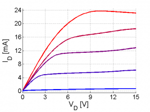
In addition to characterizing commercially available devices, GaN devices are being produced (Fig. 1) which could better meet the needs of a 400° C power converter. Room temperature operation of these devices has been demonstrated and their operating curves are shown in Fig. 2 below. By extending the known operating characteristics of the GaN devices and other circuit elements to higher temperatures, increased reliability and efficiency at this extreme operating point may be reached.

