Transfer printing of flexible hybrid inductor-capacitor filters via pre-etched silicon-on-insulator substrate
PhD student Liang Pang with Advisor K. Kim, Thin Film and Charged Particle Research Laboratory
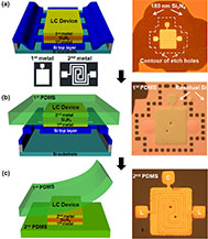
Figure 15: Illustration of the procedures used to fabricate the flexible hybrid LC filter
Flexible microelectronics and integrated circuits have important applications in paper-like displays, conformable skin sensors, and other smart systems. The transfer printing method is generally applicable for fabricating flexible electronics. It uses wet etching to remove sacrificial layers and transfers the functional layers to a flexible substrate via elastomeric stamps. Because wet etching with hydrofluoric acid (HF) is usually needed, it is difficult to use oxides or nitrides in the functional layers. The chemicals for the wet-etching process may also degrade device performance. To resolve these issues, we have developed a novel transfer-printing scheme using a pre-etched silicon-on-insulator (SOI) wafer with selectively patterned semi-stable Si-supporting membranes. This scheme facilitates both the device fabrication and transfer process and prevents the high-quality insulator deposited on the mother wafer from being subjected to HF etching. As a proof of concept, we fabricated flexible hybrid inductor-capacitor (LC) filters with large areas of functional insulator in the structure.
Figure 15 illustrates the procedures used to fabricate the hybrid LC filters and transfer them onto the elastomeric substrate. Photolithography and reactive ion etching were used to define the etch holes through the top Si and buried SiO2 (BOX) layers. The wafer was immersed in an HF solution to undercut the BOX. Since HF etching was conducted before device fabrication, the functional insulator in the structure was well protected. The top Si membranes were pulled towards the substrate by hydrophobic attraction during etching and bonded to the substrate where the BOX was completely removed. After producing the pre-etching SOI substrate, two photo-patterned metal layers were deposited by electron-beam evaporation on the Si membranes. The rectangular layer is the bottom plate of the capacitor, and the spiral layer serves as both the inductor and the top plate of the capacitor. In between, Si3N4 was deposited by plasma-enhanced chemical vapor deposition at 300 ºC as the dielectric. A flat elastomeric substrate, polydimethylsiloxane (PDMS), was brought into conformal contact with the wafer. The LC filters and the Si membranes were then peeled off the mother wafer, and the residual Si was removed by the reactive ion etcher. To facilitate testing of the dynamic response of the LC filters to mechanical stress, a more adhesive PDMS slab was used to flip over the sample. Subsequent mechanical tests demonstrated that thus-fabricated flexible LC filters are able to withstand up to 20% compressibility, in which the electronic properties varied by only 9%. This research was supported by the Grainger Center for Electric Machinery and Electromechanics and Trionix Research Lab.
This research was supported by the Grainger Center for Electric Machinery and Electromechanics.