GaN-Based MESFET with Enhaced dc Performance Using Nonalloyed Ohmic Contacts and Molecular Beam Epitaxy
Huichan (Chandler) Seo with advisers Kyekyoon (Kevin) Kim and Patrick Chapman
We previously achieved record-high peak drain current and maximum transconductance of GaN metal-semiconductor field-effect transistors (MESFETs) and extended the work to AlGaN/GaN high electron mobility transistors (HEMTs) using a selective-area-growth (SAG) technique with plasma-assisted molecular beam epitaxy (PAMBE). A KOH (heated potassium hydroxide) etching process was optimized based on the analysis of surface bonding with X-ray photoelectron spectroscopy and secondary ion mass spectroscopy (SIMS). During high-temperature annealing to alloy the metal contacts, metals react with GaN, creating a reliability problem for high-temperature device operation. To achieve high performance of electronic devices, such as HEMTs and MESFETs, a very narrow gate is needed to reduce the spacing between the source and the drain. The annealing causes severe lateral diffusion of the contact metals, making it difficult to accurately control the spacing between the source and the drain. To circumvent these problems, non-alloyed ohmic contacts are needed.
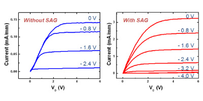
Figure 8 (a) The I-V curves and specific contact resistances of Ti, Ti/Al and Ti/Al/Ti/Au contacts, and (b) I-V characteristics of MESFET.
In our work the effects of non-alloyed ohmic contacts and surface morphology were investigated. To achieve enhanced tunneling, the SAG technique was utilized. To examine the distribution of chemical components at the interface, SIMS was used. Optimum device fabrication conditions from our previous experiments were utilized. The specific resistances of the samples with Ti, Ti/Al and Ti/Al/Ti/Au contacts were 3.5 × 10⁻⁵, 5.1 × 10⁻⁵ and 3.7 × 10⁻⁵ Ω · cm2, respectively. With the Ti contact, the GaN MESFET devices fabricated with SAG showed enhanced dc performance (Figure 8). Since annealing did not require forming the non-alloyed ohmic contacts, high-concentration silicon dopants were confined to the highly doped layers (Figure 9). We believe that fabricating highly doped layers between the contacts is essential for improved device performance, which should be facilitated by non-alloyed ohmic contacts.

Figure 9 SIMS depth profiles of Ti/Al contacts (a) with SAG and (b) without SAG.