GaN-based Flying-Capacitor Multilevel Boost Converter for High Step-Up Conversions
Zitao Liao with adviser R. Pilawa-Podgurski
The GaN-based 7-level flying-capacitor multi-level boost converter is a good solution for achieving a high boost ratio with high power density and efficiency. A converter with one-to-ten step-up with a nominal output voltage of 1 kV and a target power level of 1 kW is built to prove the concept. Figure 24 shows the topology and Figure 25 the actual hardware. The flying capacitors and inductors are placed on the bottom side of the PCB. Each flying capacitor, from C1 to C5, consists of four parallel connected ceramic capacitors. GaN switches and diodes are placed on a custom switching cell (shown in yellow) that incorporates two gate drivers and local capacitance with carefully tuned impedance to minimize ringing at switch transitions.
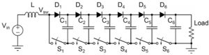
Figure 24: Converter topology
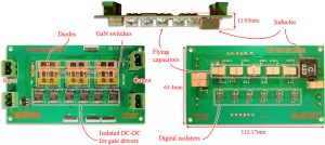
Figure 25: Converter PCB annotated
Using ceramic capacitors allows the capacitance at full rated voltage to be reduced by a factor of four to ten. This capacitance change can greatly affect balancing the flying capacitor voltages. Voltage imbalance can lead to switch failure if the switch voltage exceeds the rating. Thus the reduction of effective capacitance with increasing voltage must be taken into account at an early design stage.
Preliminary tests on the prototype converter showed that it is able to achieve 50V to 500 V at 250 W without a heatsink. A peak efficiency of 95.3 percent is attained. A number of diodes have been evaluated to further improve efficiency. Digital feedback control and an active capacitor voltage-balancing scheme are being implemented to provide a complete solution for the target application. This research is supported by the Pilawa Research Gift Account and Sandia National Laboratories.