AlGaN/GaN metal-oxide-semiconductor high-electron-mobility-transistor with high-quality gate oxide
PhD student Liang Pang with Advisor K. Kim, Thin Film and Charged Particle Research Laboratory
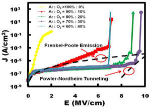
Figure 26: I-V characteristics of AI/SiO2/n+-GaN MOS-capacitors
AlGaN/GaN metal–oxide–semiconductor high-electron-mobility-transistors (MOSHEMTs) have been extensively investigated for high power microwave and switching applications. Recently, we originated an oxide deposition
scheme to deposit high-quality SiO2 on GaN. The fabricated AlGaN/GaN MOSHEMT exhibited a record high breakdown voltage per gate-drain distance of 106 V/μm. In this work, we have developed an SiO2 deposition process with the lowest thermal energy requirement among all the existing oxide deposition techniques to facilitate MOSHEMT fabrication and demonstrated GaN-MOSHEMT with a high current density and breakdown voltage.
Figure 26 shows the I-V characteristics of fabricated Al/SiO2/n+-GaN MOS-ca-pacitors with different oxygen ratios during deposition. The deposition with only argon resulted in poor-quality film with severe leakage current. However, when 10% oxygen was added into the deposition ambience, the breakdown field of the resulting SiO2 film
increased dramatically to 6.9 MV/cm, and the leakage current curve agreed well with the Poole-Frenkel model at the low electric field. A higher breakdown field and lower leakage current were achieved by further increasing the oxygen ratio, while the Fowler-Nordheim tunneling effect started to contribute to the leakage current. This indicates a reduction in defect or trap density in the film due to oxygen compensation. The largest breakdown field of 9.6 MV/cm is higher than that of the SiO2 films deposited on GaN by all other techniques including PECVD, photo-CVD,
LPD, and EB evaporation.

Figure 27: Gate leakage current as a function of reversed gate bias for SiO2/AIGaN/GaN MOSHEMT and AIGaN/GaN HEMT
Figure 27 shows the comparison of gate leakage current (Igleak) of our MOSHEMT with a conventional HEMT of the same dimension. Igleak at a reversed gate bias of -30 V for the MOSHEMT (6.5 × 10⁻⁸ A/mm) is more than four orders of magnitude lower than that of HEMT (1.6 × 10⁻³ A/mm). The maximum drain current density of the
MOSHEMT was 621 mA/mm at VGS = +4 V and the maximum transconductance (gmmax) was 73.6 mS/mm at VGS = -3 V, respectively. The three-terminal off-state breakdown voltage at VGS = -8 V was 205 V. This 205 V breakdown voltage at a gate-drain distance of 2 μm (102.5 V/μm) is higher than that of the MOSHEMTs using PECVD-SiO2, LPCVDSiO2, EB-SiO2/Gd2O3, AlN, Al2O3 or TiO2/Si3N4 as the gate insulator. Moreover, since our SiO2 deposition can be conducted at room temperature while other techniques require substrate heating during deposition, we are able to produce higher-quality SiO2 on GaN with lower thermal costs. Thus better breakdown characteristics for AlGaN/GaN MOSHEMTs can be fabricated more economically.
This research was supported by the Grainger Center for Electric Machinery and Electromechanics.