AlGaN/GaN High Electron Mobility Transistors for High Power Applications Using Selective-Area Growth by Plasma-Assisted Molecular Beam Epitaxy
Liang Pang and Huichan Seo with adviser K. Kim of the University of Illinois Thin Film and Charged Particle Research Laboratory
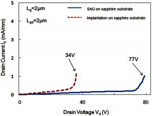
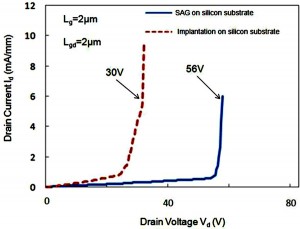
Contact resistance of GaN metal semiconductor transistors and AlGaN/GaN high electron mobility transistors (HEMTs) using a selective area growth (SAG) technique facilitated by plasma assisted molecular beam epitaxy (PAMBE) has been carried out. A heavily doped n+-GaN layer was grown only in the source/drain regions, giving rise to a record low contact resistivity of 1.8×10⁻⁸ Ώ∙cm2. The impact of SAG and ion-implantation on the electric properties of HEMTs on both sapphire and silicon substrates was compared. Samples treated with SAG showed better ohmic contacts and peak drain currents, as well as breakdown voltages about twice as high as compared with ion-implantation, as shown in Figure 13. These favorable results indicate that application of the SAG technique is suitable for fabricating HEMTs for high power applications.
A high-power HEMT using a new design is being studied. Besides utilizing SAG for current improvement, an array of HEMTs will be connected in parallel to accumulate the current. For breakdown voltage improvement, SiNx will be deposited for surface passivation. Wider gate-to-drain distance will also be employed to further enhance the breakdown behavior. Using this new design, a 3~4A current and 400~500 V breakdown voltage is expected. Thus, fabricated HEMTs will be useful for high power applications.
This research is supported by Northrup Gruman grant NRO NG 6719RO-K8A.

